× Home Services Products Catalogs Downloads TechSupport About Contact Careers (505) 872-0037

(505) 872-0037

Shopping Cart Icon
Cart
 
Login Icon
Login
Language Selector
en-be
×
Americas
Europe
Middle East & Africa
Asia Pacific & Japan
Agilent IDP-7 Dry Scroll Vacuum Pumps On Sale Agilent Varian Helium Leak Detectors On Sale Agilent IDP-10 Dry Scroll Vacuum Pumps On Sale Pfeiffer ASM340 Leak Detectors On Sale Ideal Vacuum XGC-320 Portable Digital Thermocouple Controllers On Sale Agilent TriScroll Pumps On Sale

Keyword       Part Number:      

× Vacuum Pumps Modular Vacuum Chambers Stainless Steel Vacuum Chambers Aluminum Vacuum Chambers ExploraVAC Unlimited Chambers ExploraVAC Vacuum Chambers Fittings and Flanges Feedthroughs Vacuum Valves Rebuild Kits, Parts, And Motors Vacuum Fluids, Oils, and Greases Turbo Pumps And Controllers Filters Traps and Silencers Convection and Vacuum Ovens Leak Detection and RGA Vacuum Pressure Measurement Recirculating Chillers And Water Baths
×

Load

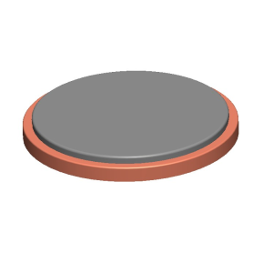
Ideal Vacuum Circular Magnetron Sputtering Targets, CHROMIUM - Cr Sputtering Target, 3'' Diameter x 0.25" Thick, 99.95 Percent Purity
Out of Stock
Expecting 2
Anticipated Arrival 2 on 2024-12-21


Ideal Vacuum Circular Magnetron Sputtering Targets, CHROMIUM - Cr Sputtering Target, 3’ Diameter x 0.25" Thick, 99.95 Percent Purity Ideal Vacuum Products, LLC. This product is a circular magnetron CHROMIUM - Cr sputtering target, with a 3’ diameter x 0.25" thickness. It is 99.95% pure. We use a very competitive pricing strategy to ensure you receive the highest quality products at the best possible value, giving you both affordability and excellence in every purchase. We offer huge discounts to every customer, customers who place bulk orders will enjoy huge savings. We stock huge quantities of our products to give our customers guaranteed same day shipping after placing an order. This short lead time is loved by all our customers who look to manage their cash flow with quicker turnaround times. Our regular customers can maintain lower inventory levels, decreasing storage costs and minimizing the risk of obsolescence. Buying from Ideal Vacuum means a customer receives their product more quickly, enhancing satisfaction and meeting their urgent needs. This also enables our customers to stay ahead of their competition by quickly adapting to new trends and demands.CHROMIUM - Cr Chromium (Cr) sputtering targets are widely used in thin-film coatings due to chromium’s excellent mechanical, chemical, and optical properties. Here’s a concise summary of chromium sputtering targets in thin-film coatings:1. Material Properties:High Hardness: Chromium is a very hard material, making it ideal for thin films that require wear resistance and durability.Corrosion Resistance: Chromium has excellent corrosion resistance, particularly in harsh environments, making it useful for protective coatings.Adhesion Promoter: Chromium thin films are often used to improve adhesion between different layers, particularly in multilayer coatings.2. Deposition Methods:DC Sputtering: Chromium is a conductive material, so DC magnetron sputtering is commonly used for deposition, ensuring high deposition rates and uniform films.RF Sputtering: RF sputtering may be used in specialized applications, particularly in reactive environments to form chromium compounds.Reactive Sputtering: Chromium is often sputtered in the presence of reactive gases (e.g., oxygen or nitrogen) to form chromium oxide (Cr2O3) or chromium nitride (CrN), which have specific uses.3. Applications:Decorative Coatings: Chromium is used in decorative thin films for items like watches, jewelry, and automotive trim due to its shiny, reflective finish and durability.Protective Coatings: Chromium thin films provide wear resistance and corrosion protection, making them ideal for tools, machinery parts, and chemical processing equipment.Microelectronics: Chromium is used in thin-film resistors, electrical contacts, and diffusion barriers in semiconductor devices due to its stability and conductivity.Optical Coatings: Chromium thin films are used in reflective coatings and anti-reflective coatings for optical devices, mirrors, and filters.Hard Coatings: Chromium compounds such as chromium nitride (CrN) are used in hard coatings for cutting tools, wear-resistant surfaces, and mechanical parts.4. Film Properties:Mechanical Strength: Chromium thin films are hard and durable, providing excellent protection in demanding applications such as tooling and industrial equipment.Corrosion Resistance: Chromium films resist oxidation and corrosion, making them ideal for protective coatings in harsh chemical environments.Adhesion: Chromium is often used as an adhesion layer in multilayer coatings, helping to bond metals, glass, and other materials.Optical Reflectivity: Chromium thin films offer good reflectivity and are used in optical and decorative coatings for their shiny metallic appearance.5. Reactive Deposition:Chromium Oxide (Cr2O3): Formed through reactive sputtering in an oxygen environment, chromium oxide is used for its hardness, wear resistance, and corrosion protection in high-performance applications.Chromium Nitride (CrN): Formed by sputtering chromium in a nitrogen atmosphere, CrN is used in hard coatings for cutting tools and other wear-resistant applications.6. Challenges:Target Poisoning: In reactive sputtering processes (e.g., forming Cr2O3 or CrN), target poisoning can occur, reducing the sputtering efficiency by forming non-metallic compounds on the target surface.Film Stress: Chromium films can develop internal stress during deposition, affecting film adhesion and mechanical properties, especially in thick layers.Summary:Chromium (Cr) sputtering targets are widely used in thin-film coatings for protective layers, decorative finishes, optical coatings, and microelectronics due to their high hardness, corrosion resistance, and excellent adhesion properties. DC sputtering is typically used for efficient chromium deposition, while reactive sputtering allows the formation of compounds like chromium oxide (Cr2O3) and chromium nitride (CrN), which are used in hard coatings for cutting tools and other demanding applications. Chromium films provide a combination of durability, protection, and reflective properties, making them versatile for a broad range of industries. Notes: Metallic or elastomer backing plate bonding is recommended for all dielectric target materials because these materials have characteristics which are not amenable to sputtering, such as, brittleness and low thermal conductivity. These targets are most susceptible to thermal shock due to their low thermal conductivity and hence, may require specific power ramp up and ramp down procedures during start up and shut down steps.

Condition: New


Part Number: P1013722


Price: €348.75


Currency: Euro (Euro)

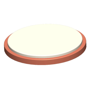
Ideal Vacuum Circular Magnetron Sputtering Targets, TITANIUM OXIDE - TiO2 Sputtering Target, 3'' Diameter x 0.125" Thick, 99.99 Percent Purity - White, Metallic Bonded to a OFHC Copper Backing Plate
Out of Stock
Expecting 2
Anticipated Arrival 2 on 2024-12-21


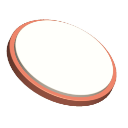
Ideal Vacuum Circular Magnetron Sputtering Targets, TITANIUM OXIDE - TiO2 Sputtering Target, 3’ Diameter x 0.125" Thick, 99.99 Percent Purity - White, Metallic Bonded to a OFHC Copper Backing Plate Ideal Vacuum Products, LLC. This product is a circular magnetron TiO2 sputtering target (white), with a 3’ diameter x 0.125" thickness. It is 99.99% pure, and is metallically bonded to a OFHC (Oxygen-Free High Conductivity) copper backing plateWe use a very competitive pricing strategy to ensure you receive the highest quality products at the best possible value, giving you both affordability and excellence in every purchase. We offer huge discounts to every customer, customers who place bulk orders will enjoy huge savings. We stock huge quantities of our products to give our customers guaranteed same day shipping after placing an order. This short lead time is loved by all our customers who look to manage their cash flow with quicker turnaround times. Our regular customers can maintain lower inventory levels, decreasing storage costs and minimizing the risk of obsolescence. Buying from Ideal Vacuum means a customer receives their product more quickly, enhancing satisfaction and meeting their urgent needs. This also enables our customers to stay ahead of their competition by quickly adapting to new trends and demands.Titanium Dioxide Titanium dioxide (TiO2) is a white, crystalline chemical compound widely used for its high refractive index and stability. It exists in three main forms: rutile, anatase, and brookite. TiO2 is primarily used as a pigment in paints, coatings, and plastics due to its excellent opacity and brightness.Titanium dioxide (white) is used in optical coatings primarily for its high refractive index, making it ideal for anti-reflective, interference, and high-reflectivity coatings. It is used in multilayer optical designs such as dielectric mirrors and filters, enhancing reflectance or transmission in specific wavelength ranges. Its stability and transparency in the visible to near-infrared spectrum also make it suitable for lenses, beam splitters, and protective coatings, where precise light control and high optical quality are required. RF vs DC Sputtering: RF sputtering is often the preferred method for sputtering pure metallic oxides because they are insulators and RF has an alternating electric field that prevents charge buildup on the target surface. This alternating field reduces the charge accumulation that would otherwise cause arcing in DC sputtering.Deposition rate: Lower deposition rate: In RF sputtering, the power transfer to the plasma is less efficient compared to DC, primarily due to the alternating nature of the electric field. This results in a lower deposition rate compared to DC sputtering under equivalent power conditions.Target Material: For conductive targets (like titanium in reactive sputtering), DC sputtering has a higher deposition rate. For insulating targets like pure metal oxides, RF sputtering must be used, and deposition rates are typically lower.Power Levels: Increasing the power can increase deposition rates in both RF and DC sputtering, but deposition rates still tend to be higher in DC for conductive materials. Pressure and Gas Flow: Higher deposition rates can be achieved by optimizing the gas pressure and flow, with different optimal conditions for RF vs. DC. Notes: Metallic or elastomer backing plate bonding is recommended for all dielectric target materials because these materials have characteristics which are not amenable to sputtering, such as, brittleness and low thermal conductivity. These targets are most susceptible to thermal shock due to their low thermal conductivity and hence, may require specific power ramp up and ramp down procedures during start up and shut down steps.

Condition: New


Part Number: P1013707


Price: €1,497.30


Currency: Euro (Euro)

Ideal Vacuum Circular Magnetron Sputtering Targets, ZIRCONIUM DIOXIDE - ZrO2 Sputtering Target, 3'' Diameter x 0.125" Thick, 99.99 Percent Purity, Metallic Bonded to a OFHC Copper Backing Plate
Out of Stock
Expecting 1
Anticipated Arrival 1 on 2024-12-21


Ideal Vacuum Circular Magnetron Sputtering Targets, ZIRCONIUM OXIDE - ZrO2 Sputtering Target, 3’ Diameter x 0.125" Thick, 99.99 Percent Purity, Metallic Bonded to a OFHC Copper Backing Plate Ideal Vacuum Products, LLC. This product is a circular magnetron ZrO2 sputtering target, with a 3’ diameter x 0.125" thickness. It is 99.99% pure, and is metallically bonded to a OFHC (Oxygen-Free High Conductivity) copper backing plateWe use a very competitive pricing strategy to ensure you receive the highest quality products at the best possible value, giving you both affordability and excellence in every purchase. We offer huge discounts to every customer, customers who place bulk orders will enjoy huge savings. We stock huge quantities of our products to give our customers guaranteed same day shipping after placing an order. This short lead time is loved by all our customers who look to manage their cash flow with quicker turnaround times. Our regular customers can maintain lower inventory levels, decreasing storage costs and minimizing the risk of obsolescence. Buying from Ideal Vacuum means a customer receives their product more quickly, enhancing satisfaction and meeting their urgent needs. This also enables our customers to stay ahead of their competition by quickly adapting to new trends and demands.Zirconium Oxide Zirconium dioxide (ZrO2), also known as zirconia, is an inorganic compound composed of zirconium and oxygen. It is a white, crystalline solid that is known for its exceptional hardness, chemical stability, and high melting point. ZrO2 is widely used in various industrial and scientific applications due to its robust physical properties and versatility.Zirconium dioxide (ZrO2) is widely used in thin film coatings for its exceptional thermal, chemical, and optical properties. Its high refractive index, chemical stability, and mechanical durability make it an ideal material for a variety of advanced thin film applications. Below are the main uses of ZrO2 in thin film coatings:1. Optical Coatings.2. Dielectric Layers.3.Protective and Barrier Coatings4. Thermal Barrier Coatings. Zirconium dioxide thin films are utilized in a wide range of advanced applications, including optical devices, microelectronics, protective coatings, and high-temperature systems, due to their unique combination of high refractive index, dielectric strength, and thermal stability. RF vs DC Sputtering: RF sputtering is often the preferred method for sputtering pure metallic oxides because they are insulators and RF has an alternating electric field that prevents charge buildup on the target surface. This alternating field reduces the charge accumulation that would otherwise cause arcing in DC sputtering.Deposition rate: Lower deposition rate: In RF sputtering, the power transfer to the plasma is less efficient compared to DC, primarily due to the alternating nature of the electric field. This results in a lower deposition rate compared to DC sputtering under equivalent power conditions.Target Material: For conductive targets (like titanium in reactive sputtering), DC sputtering has a higher deposition rate. For insulating targets like pure metal oxides, RF sputtering must be used, and deposition rates are typically lower.Power Levels: Increasing the power can increase deposition rates in both RF and DC sputtering, but deposition rates still tend to be higher in DC for conductive materials. Pressure and Gas Flow: Higher deposition rates can be achieved by optimizing the gas pressure and flow, with different optimal conditions for RF vs. DC. Notes: Metallic or elastomer backing plate bonding is recommended for all dielectric target materials because these materials have characteristics which are not amenable to sputtering, such as, brittleness and low thermal conductivity. These targets are most susceptible to thermal shock due to their low thermal conductivity and hence, may require specific power ramp up and ramp down procedures during start up and shut down steps.

Condition: New


Part Number: P1013708


Price: €1,887.90


Currency: Euro (Euro)

Ideal Vacuum Circular Magnetron Sputtering Targets, TITANIUM NITRIDE- TiN Sputtering Target, 3'' Diameter x 0.125" Thick, 99.5 Percent Purity, Metallic Bonded to a OFHC Copper Backing Plate
Out of Stock
Expecting 1
Anticipated Arrival 1 on 2024-12-21


Ideal Vacuum Circular Magnetron Sputtering Targets, TITANIUM NITRIDE- TiN Sputtering Target, 3’ Diameter x 0.125" Thick, 99.5 Percent Purity, Metallic Bonded to a OFHC Copper Backing Plate. Ideal Vacuum Products, LLC. This product is a circular magnetron TITANIUM NITRIDE- TiN sputtering target, with a 3’ diameter x 0.125" thickness. It is 99.5% pure, and is metallically bonded to a OFHC (Oxygen-Free High Conductivity) copper backing plate. We use a very competitive pricing strategy to ensure you receive the highest quality products at the best possible value, giving you both affordability and excellence in every purchase. We offer huge discounts to every customer, customers who place bulk orders will enjoy huge savings. We stock huge quantities of our products to give our customers guaranteed same day shipping after placing an order. This short lead time is loved by all our customers who look to manage their cash flow with quicker turnaround times. Our regular customers can maintain lower inventory levels, decreasing storage costs and minimizing the risk of obsolescence. Buying from Ideal Vacuum means a customer receives their product more quickly, enhancing satisfaction and meeting their urgent needs. This also enables our customers to stay ahead of their competition by quickly adapting to new trends and demands.TITANIUM NITRIDE- TiNTitanium Nitride (TiN) is a popular material for thin films due to its unique combination of mechanical, electrical, and optical properties. Here’s a summary of its key features and uses in thin films:Refractive Index: TiN has a relatively high refractive index (~2.4 to 3.0 in the visible range), making it useful for optical applications where high reflectance or specific interference effects are needed.Mechanical Properties: TiN is extremely hard and wear-resistant, with a hardness approaching that of diamond. It is commonly used as a protective coating for cutting tools, machining components, and wear-resistant surfaces.Chemical and Thermal Stability: TiN is chemically inert, corrosion-resistant, and stable at high temperatures, making it suitable for harsh environments and high-temperature applications.Electrical Conductivity: TiN is electrically conductive, which is rare for a ceramic material. This makes it useful in microelectronics as a diffusion barrier and conductive coating for components such as electrodes.Deposition Methods: TiN can be deposited using several techniques, including DC or RF sputtering, reactive sputtering (with a titanium target and nitrogen gas), and physical vapor deposition (PVD).Color and Appearance: TiN has a distinctive golden-yellow appearance, which is why it is also used for decorative coatings on jewelry and luxury items.Applications: Common in optical coatings, microelectronics, cutting tool coatings, protective layers, diffusion barriers, and decorative finishes.In summary, titanium nitride is highly valued in thin-film applications for its hardness, corrosion resistance, and electrical conductivity, making it a versatile choice in industries ranging from tooling to electronics and optics..RF vs DC Sputtering: RF sputtering is often the preferred method for sputtering pure metallic oxides because they are insulators and RF has an alternating electric field that prevents charge buildup on the target surface. This alternating field reduces the charge accumulation that would otherwise cause arcing in DC sputtering.Deposition rate: Lower deposition rate: In RF sputtering, the power transfer to the plasma is less efficient compared to DC, primarily due to the alternating nature of the electric field. This results in a lower deposition rate compared to DC sputtering under equivalent power conditions.Target Material: For conductive targets (like titanium in reactive sputtering), DC sputtering has a higher deposition rate. For insulating targets like pure metal oxides, RF sputtering must be used, and deposition rates are typically lower.Power Levels: Increasing the power can increase deposition rates in both RF and DC sputtering, but deposition rates still tend to be higher in DC for conductive materials. Pressure and Gas Flow: Higher deposition rates can be achieved by optimizing the gas pressure and flow, with different optimal conditions for RF vs. DC. Notes: Metallic or elastomer backing plate bonding is recommended for all dielectric target materials because these materials have characteristics which are not amenable to sputtering, such as, brittleness and low thermal conductivity. These targets are most susceptible to thermal shock due to their low thermal conductivity and hence, may require specific power ramp up and ramp down procedures during start up and shut down steps.

Condition: New


Part Number: P1013711


Price: €1,913.94


Currency: Euro (Euro)

Ideal Vacuum Circular Magnetron Sputtering Targets, NIOBIUM - Nb Sputtering Target, 3'' Diameter x 0.25" Thick, 99.95 Percent Purity
Out of Stock
Expecting 2
Anticipated Arrival 2 on 2024-12-21


Ideal Vacuum Circular Magnetron Sputtering Targets, NIOBIUM - Nb Sputtering Target, 3’ Diameter x 0.25" Thick, 99.95 Percent Purity. Ideal Vacuum Products, LLC. This product is a circular magnetron NIOBIUM - Nb sputtering target, with a 3’ diameter x 0.25" thickness. It is 99.95% pure. We use a very competitive pricing strategy to ensure you receive the highest quality products at the best possible value, giving you both affordability and excellence in every purchase. We offer huge discounts to every customer, customers who place bulk orders will enjoy huge savings. We stock huge quantities of our products to give our customers guaranteed same day shipping after placing an order. This short lead time is loved by all our customers who look to manage their cash flow with quicker turnaround times. Our regular customers can maintain lower inventory levels, decreasing storage costs and minimizing the risk of obsolescence. Buying from Ideal Vacuum means a customer receives their product more quickly, enhancing satisfaction and meeting their urgent needs. This also enables our customers to stay ahead of their competition by quickly adapting to new trends and demands.NIOBIUM - Nb Niobium (Nb) sputtering targets are widely used in thin-film deposition due to niobium’s unique electrical, mechanical, and superconducting properties. Here’s a concise summary of niobium sputtering targets in thin films: 1. Material Properties:High Melting Point: Niobium has a high melting point (~2477°C), making it suitable for high-temperature applications.Corrosion Resistance: Niobium is resistant to oxidation and corrosion, especially in acidic environments.Superconductivity: Niobium is a key material in superconducting applications, particularly for its high critical temperature (Tc) and ability to carry large superconducting currents.Electrical Conductivity: Niobium is a conductive material, making it useful in electronic and electrical thin-film applications.2. Deposition Methods:DC Sputtering: Since niobium is conductive, DC magnetron sputtering is commonly used, offering efficient deposition rates.RF Sputtering: RF sputtering may be used for specialized applications or in conjunction with reactive sputtering to form niobium compounds.Reactive Sputtering: Niobium can be sputtered in a reactive atmosphere (e.g., with oxygen or nitrogen) to form niobium oxide (Nb2O5) or niobium nitride (NbN) for specific applications.3. Applications:Superconducting Films: Niobium is a key material in superconducting films, which are used in superconducting quantum interference devices (SQUIDs), superconducting circuits, and particle accelerators.Microelectronics: Niobium thin films are used in capacitors, interconnects, and as diffusion barriers in microelectronics due to their excellent conductivity and stability.Optical Coatings: Niobium is used in reflective coatings and optical filters. Reactive sputtering forms niobium pentoxide (Nb2O5), which is used in high-index optical coatings.Protective Coatings: Niobium’s corrosion and oxidation resistance make it useful for protective coatings in chemical processing and high-performance applications.Niobium Nitride (NbN): Formed via reactive sputtering, NbN is used in superconducting films, hard coatings, and wear-resistant layers.4. Film Properties:Superconductivity: Niobium thin films exhibit superconductivity at low temperatures, making them essential in quantum computing and high-performance superconducting circuits.Corrosion Resistance: Niobium films provide excellent protection against corrosion, particularly in aggressive environments, making them useful for protective and barrier layers.Optical Properties: Niobium oxide (Nb2O5) films have a high refractive index (~2.2) and are used in optical coatings.Mechanical Strength: Niobium films are strong and durable, making them suitable for applications where wear resistance is needed.5. Reactive Deposition:Niobium Pentoxide (Nb2O5): Formed through reactive sputtering with oxygen, Nb2O5 is used in optical coatings, dielectrics, and capacitors due to its high dielectric constant and optical transparency.Niobium Nitride (NbN): NbN films are used in superconducting applications, as well as in hard coatings for cutting tools and wear-resistant surfaces.6. Challenges:Target Poisoning: In reactive sputtering, target poisoning can occur, where non-metallic compounds (e.g., oxides or nitrides) form on the target, reducing the sputtering efficiency.Internal Stress: Niobium films can develop internal stress during deposition, which can affect the mechanical properties and adhesion of the film.Summary:Niobium (Nb) sputtering targets are widely used in thin films for applications in superconductivity, microelectronics, optical coatings, and protective layers. DC sputtering is commonly used to deposit niobium thin films, while reactive sputtering is used to form niobium compounds like Nb2O5 (optical coatings, dielectrics) and NbN (superconducting films, hard coatings). Niobium thin films are valued for their superconducting properties, corrosion resistance, and mechanical durability across various industries. Notes: Metallic or elastomer backing plate bonding is recommended for all dielectric target materials because these materials have characteristics which are not amenable to sputtering, such as, brittleness and low thermal conductivity. These targets are most susceptible to thermal shock due to their low thermal conductivity and hence, may require specific power ramp up and ramp down procedures during start up and shut down steps.

Condition: New


Part Number: P1013719


Price: €362.70


Currency: Euro (Euro)

Ideal Vacuum Circular Magnetron Sputtering Targets, SILICON - Si (Undoped) Sputtering Target, 3'' Diameter x 0.125" Thick, 99.999 Percent Purity, Metallic Bonded to a OFHC Copper Backing Plate
Out of Stock
Expecting 2
Anticipated Arrival 2 on 2024-12-21


Ideal Vacuum Circular Magnetron Sputtering Targets, SILICON - Si (Undoped) Sputtering Target, 3’ Diameter x 0.125" Thick, 99.999 Percent Purity, Metallic Bonded to a OFHC Copper Backing Plate. Ideal Vacuum Products, LLC. This product is a circular magnetron SILICON - Si (Undoped) sputtering target, with a 3’ diameter x 0.125" thickness. It is 99.999% pure, and is metallically bonded to a OFHC (Oxygen-Free High Conductivity) copper backing plate. We use a very competitive pricing strategy to ensure you receive the highest quality products at the best possible value, giving you both affordability and excellence in every purchase. We offer huge discounts to every customer, customers who place bulk orders will enjoy huge savings. We stock huge quantities of our products to give our customers guaranteed same day shipping after placing an order. This short lead time is loved by all our customers who look to manage their cash flow with quicker turnaround times. Our regular customers can maintain lower inventory levels, decreasing storage costs and minimizing the risk of obsolescence. Buying from Ideal Vacuum means a customer receives their product more quickly, enhancing satisfaction and meeting their urgent needs. This also enables our customers to stay ahead of their competition by quickly adapting to new trends and demands.SILICON - Si (Undoped) SILICON - Si (Undoped): An undoped silicon (Si) sputtering target is widely used in various industries for thin-film deposition, particularly in semiconductors, optoelectronics, and solar cells. Here’s a summary of its key characteristics:1. Material Properties: Electrical Conductivity: Undoped silicon is a semiconductor with relatively low electrical conductivity at room temperature. It requires careful handling in applications where conductivity is important, though it becomes conductive at elevated temperatures. Purity: High-purity undoped silicon targets are often used in semiconductor applications, with typical purities exceeding 99.99% or even 99.999% for electronics-grade material. Crystalline Structure: Silicon targets can be either amorphous, polycrystalline, or single-crystal. The choice of structure affects the film’s properties, with single-crystal silicon providing superior electrical characteristics for thin-film applications.> 2. Deposition Methods: RF Sputtering: Since undoped silicon is a semiconductor, RF sputtering is typically used for thin-film deposition. This is necessary because DC sputtering would result in charge build-up on the target, making it inefficient for non-conductive or semi-conductive materials like undoped silicon. Film Quality: Films deposited using undoped silicon targets can be highly uniform and are often used in the fabrication of semiconductors, optical coatings, and photovoltaics.> 3. Applications: Microelectronics: Undoped silicon sputtering targets are essential for fabricating thin films in integrated circuits, transistors, and other semiconductor devices. Solar Cells: Thin films of undoped silicon (especially amorphous silicon or microcrystalline silicon) are used in solar cells for energy conversion. Optoelectronics: Silicon films are employed in infrared detectors, photodetectors, and MEMS devices. Passivation Layers: In semiconductor device manufacturing, silicon films are used as passivation layers or as a base material for subsequent doping or oxidation.> 4. Film Properties: Electrical Properties: Silicon films made from undoped silicon targets are intrinsic semiconductors, meaning they have low conductivity unless doped or exposed to external factors (e.g., temperature or light). Optical Properties: Undoped silicon thin films are opaque in the visible spectrum but transparent in the infrared, making them suitable for IR optics and photonic applications.> 5. Challenges: Charge Build-Up: As a semiconductor, undoped silicon cannot be efficiently sputtered using DC methods due to charge build-up on the target, so RF sputtering is essential to ensure uniform deposition. Target Quality: The purity and crystalline structure of the silicon target must be carefully controlled to avoid defects in the deposited thin films, especially for high-performance semiconductor and optical applications.> Summary:An undoped silicon sputtering target is used primarily in semiconductors, solar cells, and optoelectronics. Due to its semiconducting nature, RF sputtering is typically employed to avoid charge build-up on the target. Films produced from undoped silicon are used for their electrical, optical, and mechanical properties, with applications ranging from integrated circuits to infrared optics.. Notes: Metallic or elastomer backing plate bonding is recommended for all dielectric target materials because these materials have characteristics which are not amenable to sputtering, such as, brittleness and low thermal conductivity. These targets are most susceptible to thermal shock due to their low thermal conductivity and hence, may require specific power ramp up and ramp down procedures during start up and shut down steps.

Condition: New


Part Number: P1013716


Price: €976.50


Currency: Euro (Euro)

Ideal Vacuum Circular Magnetron Sputtering Targets, NICKEL - Ni Sputtering Target, 3'' Diameter x 0.02" Thick, 99.99 Percent Purity
Out of Stock
Expecting 2
Anticipated Arrival 2 on 2024-12-21


Ideal Vacuum Circular Magnetron Sputtering Targets, NICKEL - Ni Sputtering Target, 3’ Diameter x 0.02" Thick, 99.99 Percent Purity. Ideal Vacuum Products, LLC. This product is a circular magnetron NICKEL - Ni sputtering target, with a 3’ diameter x 0.02" thickness. It is 99.99% pure. We use a very competitive pricing strategy to ensure you receive the highest quality products at the best possible value, giving you both affordability and excellence in every purchase. We offer huge discounts to every customer, customers who place bulk orders will enjoy huge savings. We stock huge quantities of our products to give our customers guaranteed same day shipping after placing an order. This short lead time is loved by all our customers who look to manage their cash flow with quicker turnaround times. Our regular customers can maintain lower inventory levels, decreasing storage costs and minimizing the risk of obsolescence. Buying from Ideal Vacuum means a customer receives their product more quickly, enhancing satisfaction and meeting their urgent needs. This also enables our customers to stay ahead of their competition by quickly adapting to new trends and demands.NICKEL - Ni Nickel (Ni) sputtering targets are commonly used for thin-film deposition in various industrial and technological applications due to nickel’s mechanical, magnetic, and chemical properties. Here’s a concise summary of nickel sputtering targets in thin films:1. Material Properties: Magnetic Properties: Nickel is a ferromagnetic material, which makes it useful in magnetic thin-film applications such as data storage and sensors.Electrical Conductivity: Nickel is a good conductor, making it suitable for electrical and microelectronic applications.Corrosion Resistance: Nickel has excellent corrosion resistance, especially in mildly corrosive environments, making it ideal for protective coatings.2. Deposition Methods:DC Sputtering: Nickel, being a conductive material, is usually sputtered using DC magnetron sputtering, which allows for efficient deposition and higher sputtering rates.RF Sputtering: Though less common for nickel, RF sputtering can be used when required in specialized applications.Reactive Sputtering: Nickel can be sputtered in reactive environments to form nickel oxide (NiO) or other compounds for specific uses.3. Applications:Microelectronics: Nickel is used in thin-film resistors, interconnects, and contacts in semiconductor devices due to its electrical conductivity and thermal stability.Magnetic Storage Devices: Nickel is a key material in magnetic thin films for use in hard drives, magnetic sensors, and spintronic devices.Protective Coatings: Nickel thin films are often applied as corrosion-resistant coatings in industrial and chemical processing environments.Catalysts: Nickel thin films are used as catalysts in certain chemical reactions, especially in hydrogen production and fuel cells.4. Film Properties:Mechanical Strength: Nickel thin films exhibit high strength and good adhesion to various substrates, making them suitable for protective coatings.Magnetic Properties: Nickel thin films retain their magnetic properties, making them ideal for magnetic devices and sensors.Corrosion Resistance: Nickel films provide effective protection against corrosion and oxidation in various environments.Electrical Conductivity: Nickel thin films have good conductivity, making them valuable in electronics and electrical contacts.5. Reactive Deposition:Nickel Oxide (NiO): Nickel targets can be sputtered in an oxygen-rich environment to form nickel oxide films, which have applications in electrochromic devices, batteries, and gas sensors.6. Challenges:Magnetic Interference: Since nickel is a ferromagnetic material, special considerations are needed in sputtering systems to avoid interference with the magnetic field of the sputtering equipment, especially in magnetron sputtering.Stress in Thin Films: Nickel films may develop internal stress during deposition, which can impact the film’s adhesion and mechanical properties.Summary:Nickel (Ni) sputtering targets are widely used for the deposition of thin films in microelectronics, magnetic devices, and protective coatings due to nickel’s magnetic, conductive, and corrosion-resistant properties. Nickel thin films are commonly applied using DC sputtering, and they find use in electronic components, magnetic storage media, protective layers, and catalysis. Nickel oxide (NiO) films can also be created through reactive sputtering for specific functional applications. Notes: Metallic or elastomer backing plate bonding is recommended for all dielectric target materials because these materials have characteristics which are not amenable to sputtering, such as, brittleness and low thermal conductivity. These targets are most susceptible to thermal shock due to their low thermal conductivity and hence, may require specific power ramp up and ramp down procedures during start up and shut down steps.

Condition: New


Part Number: P1013718


Price: €446.40


Currency: Euro (Euro)

Ideal Vacuum Circular Magnetron Sputtering Targets, TANTALUM - Ta Sputtering Target, 3'' Diameter x 0.25" Thick, 99.95 Percent Purity
Out of Stock
Expecting 2
Anticipated Arrival 2 on 2024-12-21


Ideal Vacuum Circular Magnetron Sputtering Targets, TANTALUM - Ta Sputtering Target, 3’ Diameter x 0.25" Thick, 99.95 Percent Purity. Ideal Vacuum Products, LLC. This product is a circular magnetron TANTALUM -Ta sputtering target, with a 3’ diameter x 0.25" thickness. It is 99.95% pure. We use a very competitive pricing strategy to ensure you receive the highest quality products at the best possible value, giving you both affordability and excellence in every purchase. We offer huge discounts to every customer, customers who place bulk orders will enjoy huge savings. We stock huge quantities of our products to give our customers guaranteed same day shipping after placing an order. This short lead time is loved by all our customers who look to manage their cash flow with quicker turnaround times. Our regular customers can maintain lower inventory levels, decreasing storage costs and minimizing the risk of obsolescence. Buying from Ideal Vacuum means a customer receives their product more quickly, enhancing satisfaction and meeting their urgent needs. This also enables our customers to stay ahead of their competition by quickly adapting to new trends and demands.TANTALUM -Ta Tantalum (Ta) sputtering targets are widely used for thin-film deposition in various high-tech industries due to tantalum’s excellent mechanical, chemical, and electrical properties. Here’s a concise summary of tantalum sputtering targets in thin films:1. Material Properties:High Melting Point: Tantalum has an exceptionally high melting point (~3017 °C), making it stable under high-temperature conditions.Corrosion Resistance: Tantalum is chemically inert and highly resistant to corrosion by acids, making it ideal for protective and barrier layers.Ductility and Strength: Tantalum is both strong and ductile, allowing for the formation of durable thin films.Electrical Conductivity: Tantalum is a conductive material, which makes it suitable for use in electrical and microelectronic applications.2. Deposition Methods:DC Sputtering: Since tantalum is conductive, DC sputtering is often used for thin-film deposition, which allows for a higher deposition rate compared to RF sputtering.RF Sputtering: RF sputtering can also be used if necessary, particularly in complex deposition setups, but DC sputtering is more common for tantalum.Reactive Sputtering: Tantalum is frequently used in reactive sputtering to form tantalum compounds such as tantalum pentoxide (Ta2O5 ) for specific applications.3. Applications:Microelectronics: Tantalum is widely used in semiconductor and integrated circuit manufacturing. Thin tantalum films are employed as barrier layers in copper interconnects to prevent copper diffusion into silicon or other layers.Capacitors: Tantalum thin films are used in tantalum capacitors, where they provide high capacitance and reliability, especially in small devices.Protective Coatings: Due to its excellent corrosion resistance, tantalum is used as a protective coating in harsh chemical environments, including in the chemical processing industry and biomedical implants.Optical Coatings: Tantalum is used in some optical coatings for its mechanical strength and durability, although its primary use in optics comes from compounds like Ta2O5 .4. Film Properties:Mechanical Strength: Tantalum thin films provide strong, wear-resistant coatings, useful in protective applications.Corrosion and Oxidation Resistance: Tantalum films resist oxidation and corrosion, making them suitable for high-performance environments.Barrier Layers: Tantalum is frequently used as a diffusion barrier in microelectronics to prevent metal migration (e.g., copper) and enhance device longevity.Electrical Conductivity: Tantalum’s conductivity makes it ideal for use in electronic circuits and components, such as resistors, electrodes, and thin-film transistors.5. Reactive Deposition:Tantalum Pentoxide (Ta2O5 ): Tantalum is often sputtered in a reactive environment with oxygen to form Ta2O5 thin films, which are used in optical coatings and dielectric layers due to their high dielectric constant and optical transparency.6. Challenges:Target Poisoning: In reactive sputtering processes, target poisoning can occur when non-metallic compounds (e.g., oxides) form on the tantalum target, reducing the sputtering efficiency.Stress in Films: Tantalum films can develop internal stress during deposition, which may affect film adhesion and performance.Summary:Tantalum (Ta) sputtering targets are primarily used in microelectronics, protective coatings, and capacitors due to their high corrosion resistance, conductivity, and mechanical durability. Tantalum thin films are crucial for barrier layers in integrated circuits, diffusion barriers in copper interconnects, and in capacitor electrodes. DC sputtering is typically used for efficient deposition, while reactive sputtering can form tantalum compounds like Ta2O5 , which are widely used in optical coatings and dielectrics. Notes: Metallic or elastomer backing plate bonding is recommended for all dielectric target materials because these materials have characteristics which are not amenable to sputtering, such as, brittleness and low thermal conductivity. These targets are most susceptible to thermal shock due to their low thermal conductivity and hence, may require specific power ramp up and ramp down procedures during start up and shut down steps.

Condition: New


Part Number: P1013717


Price: €1,197.84


Currency: Euro (Euro)

Ideal Vacuum Circular Magnetron Sputtering Targets, MAGNESIUM FLUORIDE - MgF2 Sputtering Target, 3'' Diameter x 0.125" Thick, 99.995 Percent Purity, Metallic Bonded to a OFHC Copper Backing Plate
Out of Stock
Expecting 1
Anticipated Arrival 1 on 2024-12-21


Ideal Vacuum Circular Magnetron Sputtering Targets, MAGNESIUM FLUORIDE - MgF2 Sputtering Target, 3’ Diameter x 0.125" Thick, 99.995 Percent Purity, Metallic Bonded to a OFHC Copper Backing Plate Ideal Vacuum Products, LLC. This product is a circular magnetron MAGNESIUM FLUORIDE - MgF2 sputtering target, with a 3’ diameter x 0.125" thickness. It is 99.995% pure, and is metallically bonded to a OFHC (Oxygen-Free High Conductivity) copper backing plate. We use a very competitive pricing strategy to ensure you receive the highest quality products at the best possible value, giving you both affordability and excellence in every purchase. We offer huge discounts to every customer, customers who place bulk orders will enjoy huge savings. We stock huge quantities of our products to give our customers guaranteed same day shipping after placing an order. This short lead time is loved by all our customers who look to manage their cash flow with quicker turnaround times. Our regular customers can maintain lower inventory levels, decreasing storage costs and minimizing the risk of obsolescence. Buying from Ideal Vacuum means a customer receives their product more quickly, enhancing satisfaction and meeting their urgent needs. This also enables our customers to stay ahead of their competition by quickly adapting to new trends and demands.MAGNESIUM FLUORIDE - MgF2 MAGNESIUM FLUORIDE - MgF2 , is a widely used material in optical applications due to its excellent transmission properties and durability. Here’s a summary of its key characteristics: Refractive Index: ~1.38 (at 550 nm), making it a low-index material.Transparency Range: MgF2 has a broad transmission window, transmitting from the deep UV (~120 nm) to the mid-IR (~7 µm), making it suitable for UV, visible, and IR applications.Optical Coatings: Often used in anti-reflective coatings and multilayer optical coatings for lenses, filters, and other optical components.Durability: MgF2 is hard and chemically stable, resistant to environmental degradation, and suitable for use in harsh conditions.Deposition Method: Typically deposited by RF sputtering due to its insulating nature.MgF2 is commonly chosen for its wide optical transparency and low refractive index, making it ideal for reducing reflectance in various optical systems. RF vs DC Sputtering: RF sputtering is often the preferred method for sputtering pure metallic oxides because they are insulators and RF has an alternating electric field that prevents charge buildup on the target surface. This alternating field reduces the charge accumulation that would otherwise cause arcing in DC sputtering.Deposition rate: Lower deposition rate: In RF sputtering, the power transfer to the plasma is less efficient compared to DC, primarily due to the alternating nature of the electric field. This results in a lower deposition rate compared to DC sputtering under equivalent power conditions.Target Material: For conductive targets (like titanium in reactive sputtering), DC sputtering has a higher deposition rate. For insulating targets like pure metal oxides, RF sputtering must be used, and deposition rates are typically lower.Power Levels: Increasing the power can increase deposition rates in both RF and DC sputtering, but deposition rates still tend to be higher in DC for conductive materials. Pressure and Gas Flow: Higher deposition rates can be achieved by optimizing the gas pressure and flow, with different optimal conditions for RF vs. DC. Notes: Metallic or elastomer backing plate bonding is recommended for all dielectric target materials because these materials have characteristics which are not amenable to sputtering, such as, brittleness and low thermal conductivity. These targets are most susceptible to thermal shock due to their low thermal conductivity and hence, may require specific power ramp up and ramp down procedures during start up and shut down steps.

Condition: New


Part Number: P1013709


Price: €1,562.40


Currency: Euro (Euro)

Ideal Vacuum Circular Magnetron Sputtering Targets, SILICON NITRIDE- Si3N4 Sputtering Target, 3'' Diameter x 0.125" Thick, 99.5 Percent Purity, Metallic Bonded to a OFHC Copper Backing Plate
Out of Stock
Expecting 1
Anticipated Arrival 1 on 2024-12-21


Ideal Vacuum Circular Magnetron Sputtering Targets, SILICON NITRIDE- Si3N4 Sputtering Target, 3’ Diameter x 0.125" Thick, 99.5 Percent Purity, Metallic Bonded to a OFHC Copper Backing Plate Ideal Vacuum Products, LLC. This product is a circular magnetron SILICON NITRIDE- Si3N4 sputtering target, with a 3’ diameter x 0.125" thickness. It is 99.5% pure, and is metallically bonded to a OFHC (Oxygen-Free High Conductivity) copper backing plate. We use a very competitive pricing strategy to ensure you receive the highest quality products at the best possible value, giving you both affordability and excellence in every purchase. We offer huge discounts to every customer, customers who place bulk orders will enjoy huge savings. We stock huge quantities of our products to give our customers guaranteed same day shipping after placing an order. This short lead time is loved by all our customers who look to manage their cash flow with quicker turnaround times. Our regular customers can maintain lower inventory levels, decreasing storage costs and minimizing the risk of obsolescence. Buying from Ideal Vacuum means a customer receives their product more quickly, enhancing satisfaction and meeting their urgent needs. This also enables our customers to stay ahead of their competition by quickly adapting to new trends and demands.SILICON NITRIDE- Si3N4SILICON NITRIDE- Si3N4, is a versatile material used in thin-film coatings for various applications due to its mechanical, chemical, and optical properties. Here’s a summary of its key characteristics in the context of thin films: Refractive Index: ~1.9 to 2.0 (at 550 nm), making it a medium-index material often used in multilayer optical coatings.Optical Properties: Si3N4 has excellent transparency from the visible to the infrared range (~250 nm to 8 µm), making it suitable for anti-reflective coatings, waveguides, and photonics.Mechanical Properties: It is hard, wear-resistant, and has high thermal stability, making it ideal for coatings that require durability and environmental resistance.Chemical Stability: Si3N4 is chemically inert and provides good corrosion resistance, which is useful for protective coatings.Deposition Methods: Si3N4 can be deposited by RF or reactive sputtering (using a silicon target with nitrogen), as well as by PECVD (plasma-enhanced chemical vapor deposition).Applications: It is commonly used in optical coatings, semiconductor devices, protective coatings, and microelectronics due to its insulating properties and ability to act as a diffusion barrier.Si3N4 is valued for its combination of optical performance and mechanical strength, making it useful in both functional and protective thin-film coatings.RF vs DC Sputtering: RF sputtering is often the preferred method for sputtering pure metallic oxides because they are insulators and RF has an alternating electric field that prevents charge buildup on the target surface. This alternating field reduces the charge accumulation that would otherwise cause arcing in DC sputtering.Deposition rate: Lower deposition rate: In RF sputtering, the power transfer to the plasma is less efficient compared to DC, primarily due to the alternating nature of the electric field. This results in a lower deposition rate compared to DC sputtering under equivalent power conditions.Target Material: For conductive targets (like titanium in reactive sputtering), DC sputtering has a higher deposition rate. For insulating targets like pure metal oxides, RF sputtering must be used, and deposition rates are typically lower.Power Levels: Increasing the power can increase deposition rates in both RF and DC sputtering, but deposition rates still tend to be higher in DC for conductive materials. Pressure and Gas Flow: Higher deposition rates can be achieved by optimizing the gas pressure and flow, with different optimal conditions for RF vs. DC. Notes: Metallic or elastomer backing plate bonding is recommended for all dielectric target materials because these materials have characteristics which are not amenable to sputtering, such as, brittleness and low thermal conductivity. These targets are most susceptible to thermal shock due to their low thermal conductivity and hence, may require specific power ramp up and ramp down procedures during start up and shut down steps.

Condition: New


Part Number: P1013710


Price: €1,464.75


Currency: Euro (Euro)

Ideal Vacuum Circular Magnetron Sputtering Targets, TANTALUM OXIDE- Ta2O5 Sputtering Target, 3'' Diameter x 0.125" Thick, 99.995 Percent Purity, Metallic Bonded to a OFHC Copper Backing Plate
Out of Stock
Expecting 1
Anticipated Arrival 1 on 2024-12-21


Ideal Vacuum Circular Magnetron Sputtering Targets, TANTALUM OXIDE- Ta2O5 Sputtering Target, 3’ Diameter x 0.125" Thick, 99.995 Percent Purity, Metallic Bonded to a OFHC Copper Backing Plate. Ideal Vacuum Products, LLC. This product is a circular magnetron TANTALUM OXIDE- Ta2O5 sputtering target, with a 3’ diameter x 0.125" thickness. It is 99.995% pure, and is metallically bonded to a OFHC (Oxygen-Free High Conductivity) copper backing plate. We use a very competitive pricing strategy to ensure you receive the highest quality products at the best possible value, giving you both affordability and excellence in every purchase. We offer huge discounts to every customer, customers who place bulk orders will enjoy huge savings. We stock huge quantities of our products to give our customers guaranteed same day shipping after placing an order. This short lead time is loved by all our customers who look to manage their cash flow with quicker turnaround times. Our regular customers can maintain lower inventory levels, decreasing storage costs and minimizing the risk of obsolescence. Buying from Ideal Vacuum means a customer receives their product more quickly, enhancing satisfaction and meeting their urgent needs. This also enables our customers to stay ahead of their competition by quickly adapting to new trends and demands.TANTALUM OXIDE- Ta2 O5Tantalum Pentoxide Tantalum pentoxide (Ta2O5) is an inorganic compound consisting of tantalum and oxygen. It is a white, crystalline powder known for its high refractive index, excellent chemical stability, and dielectric properties. Ta2O5 is used extensively in optical and electronic applications due to its unique combination of properties. Tantalum pentoxide (Ta2O5) is widely used in thin film coatings due to its exceptional optical, electronic, and dielectric properties. Its versatility and ability to form stable, high-quality films make it ideal for a variety of high-performance applications: 1. High-Refractive Index Coatings: Ta2O5 is used in multi-layer optical coatings for lenses, mirrors, and filters. Its high refractive index helps to create precise anti-reflective and high-reflective coatings.2. Anti-Reflective Coatings: Utilized in combination with lower-refractive-index materials to produce anti-reflective coatings for enhancing light transmission in lenses and displays.3. Barrier Layers: Used as a protective layer against oxidation and corrosion in multilayer structures. 4. Electro-Optic and Photonic Devices:.Tantalum pentoxide’s unique combination of high refractive index, (~2.1 to 2.2 at 550 nm), dielectric strength, and chemical stability makes it an indispensable material in thin film coatings for optics, electronics, and photonics, enabling the development of high-performance devices and systems. Deposition Methods:Ta2O5 thin films can be deposited using RF sputtering, reactive sputtering (with tantalum and oxygen gas), and electron-beam evaporation. It is also deposited using atomic layer deposition (ALD) for precise, conformal coatings in microelectronics. Notes: Metallic or elastomer backing plate bonding is recommended for all dielectric target materials because these materials have characteristics which are not amenable to sputtering, such as, brittleness and low thermal conductivity. These targets are most susceptible to thermal shock due to their low thermal conductivity and hence, may require specific power ramp up and ramp down procedures during start up and shut down steps.

Condition: New


Part Number: P1013712


Price: €1,841.40


Currency: Euro (Euro)

Ideal Vacuum Circular Magnetron Sputtering Targets, ALUMINUM OXIDE- Al2O3 Sputtering Target, 3'' Diameter x 0.125" Thick, 99.99 Percent Purity, Metallic Bonded to a OFHC Copper Backing Plate
Out of Stock
Expecting 1
Anticipated Arrival 1 on 2024-12-21


Ideal Vacuum Circular Magnetron Sputtering Targets, ALUMINUM OXIDE- Al2O3 Sputtering Target, 3’ Diameter x 0.125" Thick, 99.99 Percent Purity, Metallic Bonded to a OFHC Copper Backing Plate. Ideal Vacuum Products, LLC. This product is a circular magnetron ALUMINUM OXIDE- Al2O3 sputtering target, with a 3’ diameter x 0.125" thickness. It is 99.99% pure, and is metallically bonded to a OFHC (Oxygen-Free High Conductivity) copper backing plate. We use a very competitive pricing strategy to ensure you receive the highest quality products at the best possible value, giving you both affordability and excellence in every purchase. We offer huge discounts to every customer, customers who place bulk orders will enjoy huge savings. We stock huge quantities of our products to give our customers guaranteed same day shipping after placing an order. This short lead time is loved by all our customers who look to manage their cash flow with quicker turnaround times. Our regular customers can maintain lower inventory levels, decreasing storage costs and minimizing the risk of obsolescence. Buying from Ideal Vacuum means a customer receives their product more quickly, enhancing satisfaction and meeting their urgent needs. This also enables our customers to stay ahead of their competition by quickly adapting to new trends and demands.ALUMINUM OXIDE- Al2O31. Refractive Index: Refractive Index: ~1.63 (at 550 nm), making it a low to medium-index material. This property makes it suitable for use in multilayer optical coatings, such as anti-reflective coatings, dielectric mirrors, and filters.2. Optical Transparency: Transmission Window: Al2O3 is highly transparent from the ultraviolet (UV) to the infrared (IR) range, from ~200 nm to ~5 µm. This makes it suitable for a variety of optical applications in UV, visible, and IR wavelengths.3. Mechanical Properties: Al2O3 is extremely hard and wear-resistant, making it an excellent choice for protective coatings and abrasion-resistant layers on surfaces subject to mechanical stress. Its high mechanical strength also makes it suitable for microelectronic and protective coatings in harsh environments.4. Chemical and Thermal Stability: Al2O3 is highly chemically inert and resistant to corrosion and oxidation, making it suitable for use in chemically harsh environments. It has high thermal stability, making it useful in high-temperature applications.5. Dielectric Properties: High Dielectric Constant: Al2O3 has a relatively high dielectric constant (~9), which makes it useful as a gate dielectric and in capacitors for electronic applications. It serves as an excellent insulating layer in semiconductor devices, providing good electrical insulation and thermal stability.6. Deposition Methods: Al2O3 thin films can be deposited by a variety of methods, including RF sputtering, reactive sputtering, atomic layer deposition (ALD), and thermal evaporation. ALD is particularly favored for ultra-thin, conformal coatings in semiconductor and nanotechnology applications.7. Applications: Optical Coatings: Al2O3 is commonly used in anti-reflective coatings, protective coatings on optics, and as a part of multilayer dielectric mirrors. Microelectronics: Al2O3 is widely used in MOSFETs as a gate insulator, in capacitors, and as a passivation layer in semiconductor devices. Protective Coatings: Due to its hardness and resistance to wear and chemicals, it is used to protect surfaces in industrial applications. Barrier Coatings: Al2O3 provides an excellent diffusion barrier and is used in packaging and moisture protection layers.Summary:Aluminum Oxide (Al2O3 ) is a versatile material in thin films, offering optical transparency, mechanical durability, chemical inertness, and dielectric properties. It is widely used in optical coatings, microelectronics, protective layers, and barrier coatings, with applications ranging from semiconductor devices to abrasion-resistant coatings and optical elements. Its combination of transparency and stability makes it a critical material for high-performance coatings across various industries. Notes: Metallic or elastomer backing plate bonding is recommended for all dielectric target materials because these materials have characteristics which are not amenable to sputtering, such as, brittleness and low thermal conductivity. These targets are most susceptible to thermal shock due to their low thermal conductivity and hence, may require specific power ramp up and ramp down procedures during start up and shut down steps.

Condition: New


Part Number: P1013714


Price: €1,165.29


Currency: Euro (Euro)

Ideal Vacuum Circular Magnetron Sputtering Targets, SILICON DIOXIDE- SiO2 Sputtering Target, 3'' Diameter x 0.125" Thick, 99.995 Percent Purity, Metallic Bonded to a OFHC Copper Backing Plate
Out of Stock
Expecting 1
Anticipated Arrival 1 on 2024-12-21


Ideal Vacuum Circular Magnetron Sputtering Targets, SILICON DIOXIDE- SiO2 Sputtering Target, 3’ Diameter x 0.125" Thick, 99.995 Percent Purity, Metallic Bonded to a OFHC Copper Backing Plate. Ideal Vacuum Products, LLC. This product is a circular magnetron SILICON DIOXIDE- SiO2 sputtering target, with a 3’ diameter x 0.125" thickness. It is 99.995% pure, and is metallically bonded to a OFHC (Oxygen-Free High Conductivity) copper backing plate. We use a very competitive pricing strategy to ensure you receive the highest quality products at the best possible value, giving you both affordability and excellence in every purchase. We offer huge discounts to every customer, customers who place bulk orders will enjoy huge savings. We stock huge quantities of our products to give our customers guaranteed same day shipping after placing an order. This short lead time is loved by all our customers who look to manage their cash flow with quicker turnaround times. Our regular customers can maintain lower inventory levels, decreasing storage costs and minimizing the risk of obsolescence. Buying from Ideal Vacuum means a customer receives their product more quickly, enhancing satisfaction and meeting their urgent needs. This also enables our customers to stay ahead of their competition by quickly adapting to new trends and demands.SILICON DIOXIDE - SiO2 Silicon Dioxide (SiO2 ) is one of the most commonly used materials in thin-film coatings due to its excellent optical, dielectric, and protective properties. Here’s a concise summary of SiO2 in thin films:1. Refractive Index: Refractive Index: ~1.45 (at 550 nm), making it a low-index material. It is widely used in optical coatings, such as anti-reflective coatings and dielectric mirrors, where a low refractive index layer is required.2. Optical Transparency: Transmission Window: SiO2 has a broad transparency range, from the ultraviolet (UV) (~160 nm) to the infrared (IR) (~2.5 µm). This makes it an ideal material for coatings in the visible, UV, and IR spectral ranges.3. Dielectric Properties: Low Dielectric Constant: SiO2 has a relatively low dielectric constant (~3.9), which makes it useful as an insulating layer in microelectronics and semiconductors. It serves as an effective dielectric barrier in devices like MOSFETs.4. Chemical and Thermal Stability: SiO2 is chemically inert, making it highly resistant to corrosion and oxidation. It has excellent thermal stability, allowing it to withstand high temperatures in various applications.5. Mechanical Properties: SiO2 is hard and offers good abrasion resistance, making it a protective material in thin-film coatings. However, it is brittle, and care must be taken in applications involving mechanical stress.6. Deposition Methods: SiO2 thin films can be deposited using various techniques, including RF sputtering, chemical vapor deposition (CVD), thermal evaporation, and electron-beam deposition. RF sputtering is commonly used for thin, uniform coatings of SiO2 .7. Applications: Optical Coatings: SiO2 is widely used in anti-reflective coatings, high/low index multilayer coatings, and as protective coatings for optics. Microelectronics: SiO2 serves as an insulating layer in integrated circuits, passivation layers, and as a gate oxide in MOSFETs. Protective Coatings: Due to its chemical stability and hardness, SiO2 is used in protective and wear-resistant coatings. Barrier Layers: SiO2 is effective as a diffusion barrier and moisture protection layer in various applications.Summary: SiO2 is a low-refractive-index material with broad optical transparency, excellent dielectric properties, and strong chemical stability, making it highly versatile in optical coatings, electronics, and protective layers. Its durability and wide transmission range are key factors in its broad use in thin films across industries. Notes: Metallic or elastomer backing plate bonding is recommended for all dielectric target materials because these materials have characteristics which are not amenable to sputtering, such as, brittleness and low thermal conductivity. These targets are most susceptible to thermal shock due to their low thermal conductivity and hence, may require specific power ramp up and ramp down procedures during start up and shut down steps.

Condition: New


Part Number: P1013715


Price: €846.30


Currency: Euro (Euro)

Ideal Vacuum Circular Magnetron Sputtering Targets, NIOBIUM OXIDE- Nb2O5 Sputtering Target, 3'' Diameter x 0.125" Thick, 99.995 Percent Purity, Metallic Bonded to a OFHC Copper Backing Plate
Out of Stock
Expecting 1
Anticipated Arrival 1 on 2024-12-21


Ideal Vacuum Circular Magnetron Sputtering Targets, NIOBIUM OXIDE- Nb2O5 Sputtering Target, 3’ Diameter x 0.125" Thick, 99.995 Percent Purity, Metallic Bonded to a OFHC Copper Backing Plate. Ideal Vacuum Products, LLC. This product is a circular magnetron NIOBIUM OXIDE- Nb2O5 sputtering target, with a 3’ diameter x 0.125" thickness. It is 99.995% pure, and is metallically bonded to a OFHC (Oxygen-Free High Conductivity) copper backing plate. We use a very competitive pricing strategy to ensure you receive the highest quality products at the best possible value, giving you both affordability and excellence in every purchase. We offer huge discounts to every customer, customers who place bulk orders will enjoy huge savings. We stock huge quantities of our products to give our customers guaranteed same day shipping after placing an order. This short lead time is loved by all our customers who look to manage their cash flow with quicker turnaround times. Our regular customers can maintain lower inventory levels, decreasing storage costs and minimizing the risk of obsolescence. Buying from Ideal Vacuum means a customer receives their product more quickly, enhancing satisfaction and meeting their urgent needs. This also enables our customers to stay ahead of their competition by quickly adapting to new trends and demands.NIOBIUM OXIDE- Nb2O5Niobium Oxide (Nb2O5) is a valuable material for thin films due to its excellent optical, dielectric, and catalytic properties. Here’s a summary of its key characteristics: 1. Refractive Index: Refractive Index: ~2.2 to 2.4 (at 550 nm), making it a high-index material. Its high refractive index makes it ideal for optical coatings, especially in multilayer structures like anti-reflective coatings, optical filters, and waveguides.2. Optical Transparency: Transmission Window: Nb2O5 is transparent from the visible to the infrared range (~400 nm to 5 µm), making it suitable for a wide range of optical applications. It is commonly used in optical coatings for lenses, mirrors, and photonic devices.3. Dielectric Properties: High Dielectric Constant: Nb2O5 has a high dielectric constant (20-40), which makes it useful in capacitors, memory devices, and other electronic components requiring high capacitance. It is also utilized as a gate dielectric material in thin-film transistors.4. Chemical and Thermal Stability: Nb2O5 is chemically stable and resistant to corrosion. It offers excellent stability under high temperatures, making it a reliable material for thin films used in demanding environments. Its thermal stability ensures its performance in applications exposed to high temperatures.5. Mechanical Properties: Nb2O5 is hard and durable, providing excellent mechanical strength to thin-film coatings, making it useful for protective coatings and abrasion-resistant layers.6. Deposition Methods: Nb2O5 thin films can be deposited using various techniques, including RF sputtering, reactive sputtering (using niobium metal with oxygen gas), thermal evaporation, and electron-beam evaporation. It can also be deposited by atomic layer deposition (ALD) for high-precision thin films.7. Applications: Optical Coatings: Used in anti-reflective coatings, optical filters, and waveguides due to its high refractive index and transparency. Microelectronics: Nb2O5 is employed in capacitors, thin-film transistors, and as a high-k dielectric material in semiconductor devices.Catalysis: Nb2O5 is also known for its catalytic properties and is used in applications such as photocatalysis and fuel cells.Protective Coatings: Provides excellent wear resistance and corrosion protection in industrial applications.Summary: Niobium Pentoxide (Nb2O5) is a high-refractive-index material with excellent optical and dielectric properties, making it a popular choice for optical coatings and electronic applications. Its chemical stability, dielectric constant, and high transparency make it suitable for a variety of thin-film applications, including capacitors, anti-reflective coatings, and photonic devices. Notes: Metallic or elastomer backing plate bonding is recommended for all dielectric target materials because these materials have characteristics which are not amenable to sputtering, such as, brittleness and low thermal conductivity. These targets are most susceptible to thermal shock due to their low thermal conductivity and hence, may require specific power ramp up and ramp down procedures during start up and shut down steps.

Condition: New


Part Number: P1013713


Price: €898.38


Currency: Euro (Euro)

Ideal Vacuum Circular Magnetron Sputtering Targets, TITANIUM - Ti Sputtering Target, 3'' Diameter x 0.25" Thick, 99.995 Percent Purity
Out of Stock
Expecting 2
Anticipated Arrival 2 on 2024-12-21


Ideal Vacuum Circular Magnetron Sputtering Targets, TITANIUM - Ti Sputtering Target, 3’ Diameter x 0.25" Thick, 99.995 Percent Purity Ideal Vacuum Products, LLC. This product is a circular magnetron TITANIUM - Ti sputtering target, with a 3’ diameter x 0.25" thickness. It is 99.995% pure. We use a very competitive pricing strategy to ensure you receive the highest quality products at the best possible value, giving you both affordability and excellence in every purchase. We offer huge discounts to every customer, customers who place bulk orders will enjoy huge savings. We stock huge quantities of our products to give our customers guaranteed same day shipping after placing an order. This short lead time is loved by all our customers who look to manage their cash flow with quicker turnaround times. Our regular customers can maintain lower inventory levels, decreasing storage costs and minimizing the risk of obsolescence. Buying from Ideal Vacuum means a customer receives their product more quickly, enhancing satisfaction and meeting their urgent needs. This also enables our customers to stay ahead of their competition by quickly adapting to new trends and demands.TITANIUM - Ti Titanium (Ti) sputtering targets are widely used in thin-film deposition due to titanium’s excellent mechanical, chemical, and physical properties. Here’s a summary of titanium sputtering targets in thin films:1. Material Properties:High Strength-to-Weight Ratio: Titanium is known for its light weight and high mechanical strength, making it ideal for thin films that require durability without adding significant mass.Corrosion Resistance: Titanium is highly resistant to corrosion, especially in harsh environments such as seawater and acidic conditions.Biocompatibility: Titanium is biocompatible, which makes it suitable for use in medical devices and biomedical coatings.2. Deposition Methods:DC Sputtering: Titanium is a conductive material, so DC magnetron sputtering is commonly used for efficient thin-film deposition.RF Sputtering: RF sputtering can be used in cases where reactive sputtering or more complex thin-film structures are required.Reactive Sputtering: Titanium is frequently sputtered in the presence of reactive gases (such as oxygen or nitrogen) to form titanium compounds like titanium dioxide (TiO2) and titanium nitride (TiN).3. Applications:Microelectronics: Titanium is used in diffusion barriers, adhesion layers, and electrical contacts in semiconductor devices. It forms thin films that help prevent metal diffusion in integrated circuits.Optical Coatings: Titanium is used in optical coatings, particularly in anti-reflective coatings, as a durable protective layer. Titanium dioxide (TiO2) is a high-refractive-index material often used in multilayer optical coatings.Protective Coatings: Titanium thin films are commonly used for corrosion-resistant and wear-resistant coatings in aerospace, automotive, and chemical industries.Medical Applications: Due to its biocompatibility, titanium is used in thin films for implants, prosthetics, and medical devices to improve their durability and interaction with biological tissues.Catalysis: Titanium-based thin films (such as TiO2) are used in photocatalysis, particularly in environmental applications like air and water purification.4. Film Properties:Mechanical Strength: Titanium films are known for their durability and strength, providing wear resistance and mechanical protection.Corrosion Resistance: Thin films of titanium are highly resistant to corrosion, making them ideal for use in marine environments and other aggressive chemical conditions.Adhesion: Titanium thin films often serve as adhesion layers to improve the bonding of other coatings, especially on materials that don’t naturally bond well.Optical Properties: Titanium dioxide (TiO2) films, formed through reactive sputtering, are highly transparent in the visible range and have a high refractive index (~2.5), making them suitable for optical coatings.5. Reactive Deposition:Titanium Dioxide (TiO2): Formed through reactive sputtering in an oxygen environment, TiO2 is used in optical coatings, solar cells, and photocatalysts due to its transparency and high refractive index.Titanium Nitride (TiN): Formed by sputtering titanium in a nitrogen atmosphere, TiN is used in hard coatings, wear-resistant surfaces, and conductive films in microelectronics.6. Challenges:Oxidation: Titanium is reactive, and care must be taken to control the oxidation state, especially during deposition in reactive environments (e.g., forming TiO2 without over-oxidizing the film).Stress in Films: Titanium thin films can develop internal stress during deposition, which may affect film adhesion and mechanical properties.Summary:Titanium (Ti) sputtering targets are widely used in microelectronics, optical coatings, protective layers, and medical devices due to titanium’s high strength, corrosion resistance, and biocompatibility. DC sputtering is commonly used for titanium deposition, while reactive sputtering allows the formation of titanium compounds like TiO2 and TiN, which have applications in optics, photocatalysis, and hard coatings. Titanium thin films provide excellent mechanical strength, corrosion resistance, and adhesion properties across a broad range of industries. Notes: Metallic or elastomer backing plate bonding is recommended for all dielectric target materials because these materials have characteristics which are not amenable to sputtering, such as, brittleness and low thermal conductivity. These targets are most susceptible to thermal shock due to their low thermal conductivity and hence, may require specific power ramp up and ramp down procedures during start up and shut down steps.

Condition: New


Part Number: P1013721


Price: €232.50


Currency: Euro (Euro)

Ideal Vacuum Circular Magnetron Sputtering Targets, COPPER - Cu Sputtering Target or Cu Backing Plate, 3'' Diameter x 0.25" Thick, 99.99 Percent Purity
Out of Stock
Expecting 2
Anticipated Arrival 2 on 2024-12-21


Ideal Vacuum Circular Magnetron Sputtering Targets, COPPER - Cu Sputtering Target or Cu Backing Plate, 3’ Diameter x 0.25" Thick, 99.99 Percent Purity Ideal Vacuum Products, LLC. This product is a circular magnetron COPPER - Cu sputtering target, or Cu backing plate, with a 3’ diameter x 0.25" thickness. It is 99.99% pure. We use a very competitive pricing strategy to ensure you receive the highest quality products at the best possible value, giving you both affordability and excellence in every purchase. We offer huge discounts to every customer, customers who place bulk orders will enjoy huge savings. We stock huge quantities of our products to give our customers guaranteed same day shipping after placing an order. This short lead time is loved by all our customers who look to manage their cash flow with quicker turnaround times. Our regular customers can maintain lower inventory levels, decreasing storage costs and minimizing the risk of obsolescence. Buying from Ideal Vacuum means a customer receives their product more quickly, enhancing satisfaction and meeting their urgent needs. This also enables our customers to stay ahead of their competition by quickly adapting to new trends and demands.COPPER - Cu Copper (Cu) sputtering targets are commonly used in thin-film deposition due to copper’s excellent electrical and thermal properties. Here’s a concise summary of copper sputtering targets in thin films:1. Material Properties:High Electrical Conductivity: Copper is one of the best conductors of electricity, making it ideal for thin films in microelectronics and electrical applications.Thermal Conductivity: Copper has high thermal conductivity, making it valuable for thin films where heat dissipation is critical.Ductility: Copper is a ductile material, meaning it can form thin films that are mechanically stable and flexible.2. Deposition Methods:DC Sputtering: Since copper is a conductive material, DC magnetron sputtering is commonly used for efficient thin-film deposition.RF Sputtering: Although DC sputtering is preferred, RF sputtering can also be used for certain applications where alternating fields are necessary.Reactive Sputtering: Copper can be sputtered in reactive environments with gases like oxygen to form copper oxides (e.g., CuO, Cu2O) for specific applications.3. Applications:Microelectronics: Copper is extensively used in integrated circuits, semiconductor devices, and thin-film transistors as interconnects and electrical contacts due to its superior electrical conductivity.Printed Circuit Boards (PCBs): Thin films of copper are crucial in the manufacture of PCBs, where they form conductive pathways for electronic components.Solar Cells: Copper is used in some thin-film solar cells for electrical contacts and as a component in compounds like CIGS (copper indium gallium selenide).Optical Coatings: Copper is occasionally used in reflective coatings and mirrors due to its high reflectivity in the visible and infrared ranges.Heat Sinks and Thermal Management: Copper thin films are used in applications where thermal conductivity is essential, such as heat sinks and thermal management layers in microelectronics.4. Film Properties:High Electrical Conductivity: Copper thin films have excellent electrical properties, making them ideal for conductive layers in electronics.Thermal Conductivity: Copper films efficiently dissipate heat, improving device reliability and longevity in high-power electronic applications.Corrosion Resistance: Copper films can be susceptible to oxidation, so protective layers (like nickel or chromium) are often added to prevent corrosion.Adhesion: Copper has good adhesion to a variety of substrates, but adhesion layers (like titanium or chromium) are sometimes used to enhance bonding with certain materials.5. Reactive Deposition:Copper Oxides (CuO, Cu2O): Copper can be sputtered in an oxygen-rich environment to form copper oxides, which have applications in electronics, sensors, and photovoltaics due to their semiconducting properties.6. Challenges:Oxidation: Copper is prone to oxidation, especially in the presence of air or moisture. To avoid this, deposition is often done in a controlled environment, and additional protective layers may be applied.Electromigration: In microelectronics, thin copper films can experience electromigration, where atoms move under the influence of an electrical current, potentially leading to device failure. Barrier layers (e.g., tantalum or titanium) are used to mitigate this effect.Diffusion: Copper can diffuse into other materials, particularly silicon, which can degrade device performance. Diffusion barriers (like tantalum) are used to prevent this.Summary: Copper (Cu) sputtering targets are essential for thin-film applications in microelectronics, solar cells, optical coatings, and thermal management due to copper’s high electrical conductivity, thermal conductivity, and ductility. DC sputtering is commonly used for copper deposition, and reactive sputtering can create copper oxides for specialized applications. Copper thin films are widely used for interconnects, electrical contacts, and heat dissipation, though care must be taken to prevent oxidation and diffusion in sensitive applications. Notes: Metallic or elastomer backing plate bonding is recommended for all dielectric target materials because these materials have characteristics which are not amenable to sputtering, such as, brittleness and low thermal conductivity. These targets are most susceptible to thermal shock due to their low thermal conductivity and hence, may require specific power ramp up and ramp down procedures during start up and shut down steps.

Condition: New


Part Number: P1013723


Price: €186.00


Currency: Euro (Euro)
Marca de agua con el logotipo de Ideal Vacuum
CONTACT US
Ideal Vacuum Products , LLC
5910 Midway Park Blvd NE
Albuquerque, New Mexico 87109-5805 USA

Phone: (505) 872-0037
Fax: (505) 872-9001
info@idealvac.com