× Home Services Products Catalogs Downloads TechSupport About Contact Careers (505) 872-0037

(505) 872-0037

Shopping Cart Icon
Cart
 
Login Icon
Login
Language Selector
en-pr
×
Americas
Europe
Middle East & Africa
Asia Pacific & Japan
Agilent IDP-10 Dry Scroll Vacuum Pumps On Sale Pfeiffer ASM340 Leak Detectors On Sale Ideal Vacuum XG-120 Digital Thermocouple Gauges On Sale Agilent IDP-15 Dry Scroll Vacuum Pumps On Sale Agilent IDP-7 Dry Scroll Vacuum Pumps On Sale Agilent TriScroll Pumps On Sale

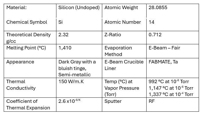
Keyword       Part Number:      

× Vacuum Pumps Modular Vacuum Chambers Stainless Steel Vacuum Chambers Aluminum Vacuum Chambers ExploraVAC Unlimited Chambers ExploraVAC Vacuum Chambers Fittings and Flanges Feedthroughs Vacuum Valves Rebuild Kits, Parts, And Motors Vacuum Fluids, Oils, and Greases Turbo Pumps And Controllers Filters Traps and Silencers Convection and Vacuum Ovens Leak Detection and RGA Vacuum Pressure Measurement Recirculating Chillers And Water Baths
×

Load

Product Image 1
Product Image 2
Product Image 3
NEW ITEM

Ideal Vacuum Circular Magnetron Sputtering Targets, SILICON - Si (Undoped) Sputtering Target, 3'' Diameter x 0.125" Thick, 99.999 Percent Purity, Metallic Bonded to a OFHC Copper Backing Plate

Condition:
  New
Part Number:
  P1013716
Warranty:
  Full Manufacturer's Warranty

Out of Stock   

Sale: $1,125.00

Ideal Vacuum Circular Magnetron Sputtering Targets, SILICON - Si (Undoped) Sputtering Target, 3'' Diameter x 0.125" Thick, 99.999 Percent Purity, Metallic Bonded to a OFHC Copper Backing Plate 1125
Currency: US Dollar (USD)

Description

Ideal Vacuum Circular Magnetron Sputtering Targets, SILICON - Si (Undoped) Sputtering Target, 3'' Diameter x 0.125" Thick, 99.999 Percent Purity, Metallic Bonded to a OFHC Copper Backing Plate.
Ideal Vacuum Products, LLC.

This product is a circular magnetron SILICON - Si (Undoped) sputtering target, with a 3'' diameter x 0.125" thickness. It is 99.999% pure, and is metallically bonded to a OFHC (Oxygen-Free High Conductivity) copper backing plate.

We use a very competitive pricing strategy to ensure you receive the highest quality products at the best possible value, giving you both affordability and excellence in every purchase. We offer huge discounts to every customer, customers who place bulk orders will enjoy huge savings. We stock huge quantities of our products to give our customers guaranteed same day shipping after placing an order. This short lead time is loved by all our customers who look to manage their cash flow with quicker turnaround times. Our regular customers can maintain lower inventory levels, decreasing storage costs and minimizing the risk of obsolescence. Buying from Ideal Vacuum means a customer receives their product more quickly, enhancing satisfaction and meeting their urgent needs. This also enables our customers to stay ahead of their competition by quickly adapting to new trends and demands.

SILICON - Si (Undoped)

SILICON - Si (Undoped): An undoped silicon (Si) sputtering target is widely used in various industries for thin-film deposition, particularly in semiconductors, optoelectronics, and solar cells. Here’s a summary of its key characteristics:

1. Material Properties: Electrical Conductivity: Undoped silicon is a semiconductor with relatively low electrical conductivity at room temperature. It requires careful handling in applications where conductivity is important, though it becomes conductive at elevated temperatures. Purity: High-purity undoped silicon targets are often used in semiconductor applications, with typical purities exceeding 99.99% or even 99.999% for electronics-grade material. Crystalline Structure: Silicon targets can be either amorphous, polycrystalline, or single-crystal. The choice of structure affects the film's properties, with single-crystal silicon providing superior electrical characteristics for thin-film applications.>

2. Deposition Methods: RF Sputtering: Since undoped silicon is a semiconductor, RF sputtering is typically used for thin-film deposition. This is necessary because DC sputtering would result in charge build-up on the target, making it inefficient for non-conductive or semi-conductive materials like undoped silicon. Film Quality: Films deposited using undoped silicon targets can be highly uniform and are often used in the fabrication of semiconductors, optical coatings, and photovoltaics.>

3. Applications: Microelectronics: Undoped silicon sputtering targets are essential for fabricating thin films in integrated circuits, transistors, and other semiconductor devices. Solar Cells: Thin films of undoped silicon (especially amorphous silicon or microcrystalline silicon) are used in solar cells for energy conversion. Optoelectronics: Silicon films are employed in infrared detectors, photodetectors, and MEMS devices. Passivation Layers: In semiconductor device manufacturing, silicon films are used as passivation layers or as a base material for subsequent doping or oxidation.>

4. Film Properties: Electrical Properties: Silicon films made from undoped silicon targets are intrinsic semiconductors, meaning they have low conductivity unless doped or exposed to external factors (e.g., temperature or light). Optical Properties: Undoped silicon thin films are opaque in the visible spectrum but transparent in the infrared, making them suitable for IR optics and photonic applications.>

5. Challenges: Charge Build-Up: As a semiconductor, undoped silicon cannot be efficiently sputtered using DC methods due to charge build-up on the target, so RF sputtering is essential to ensure uniform deposition. Target Quality: The purity and crystalline structure of the silicon target must be carefully controlled to avoid defects in the deposited thin films, especially for high-performance semiconductor and optical applications.>

Summary:
An undoped silicon sputtering target is used primarily in semiconductors, solar cells, and optoelectronics. Due to its semiconducting nature, RF sputtering is typically employed to avoid charge build-up on the target. Films produced from undoped silicon are used for their electrical, optical, and mechanical properties, with applications ranging from integrated circuits to infrared optics..


Notes:
Metallic or elastomer backing plate bonding is recommended for all dielectric target materials because these materials have characteristics which are not amenable to sputtering, such as, brittleness and low thermal conductivity. These targets are most susceptible to thermal shock due to their low thermal conductivity and hence, may require specific power ramp up and ramp down procedures during start up and shut down steps.

Downloads

Marca de agua con el logotipo de Ideal Vacuum
CONTACT US
Ideal Vacuum Products , LLC
5910 Midway Park Blvd NE
Albuquerque, New Mexico 87109-5805 USA

Phone: (505) 872-0037
Fax: (505) 872-9001
info@idealvac.com


Press ESC to Close


deepbox image 2
load time = 0.9004