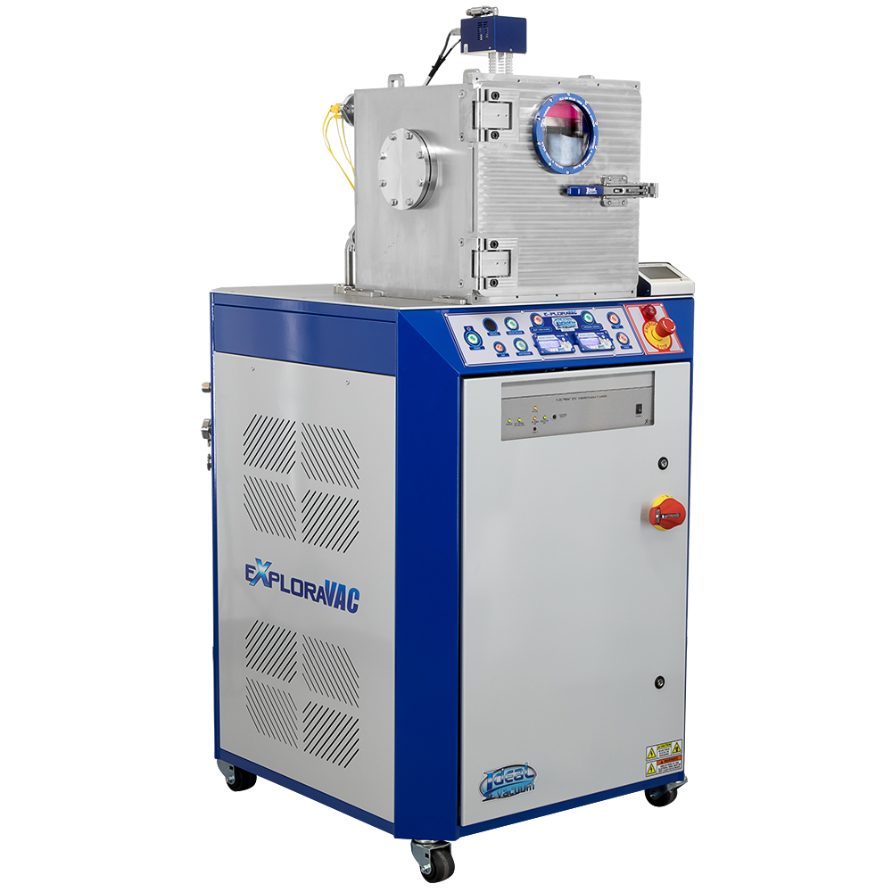
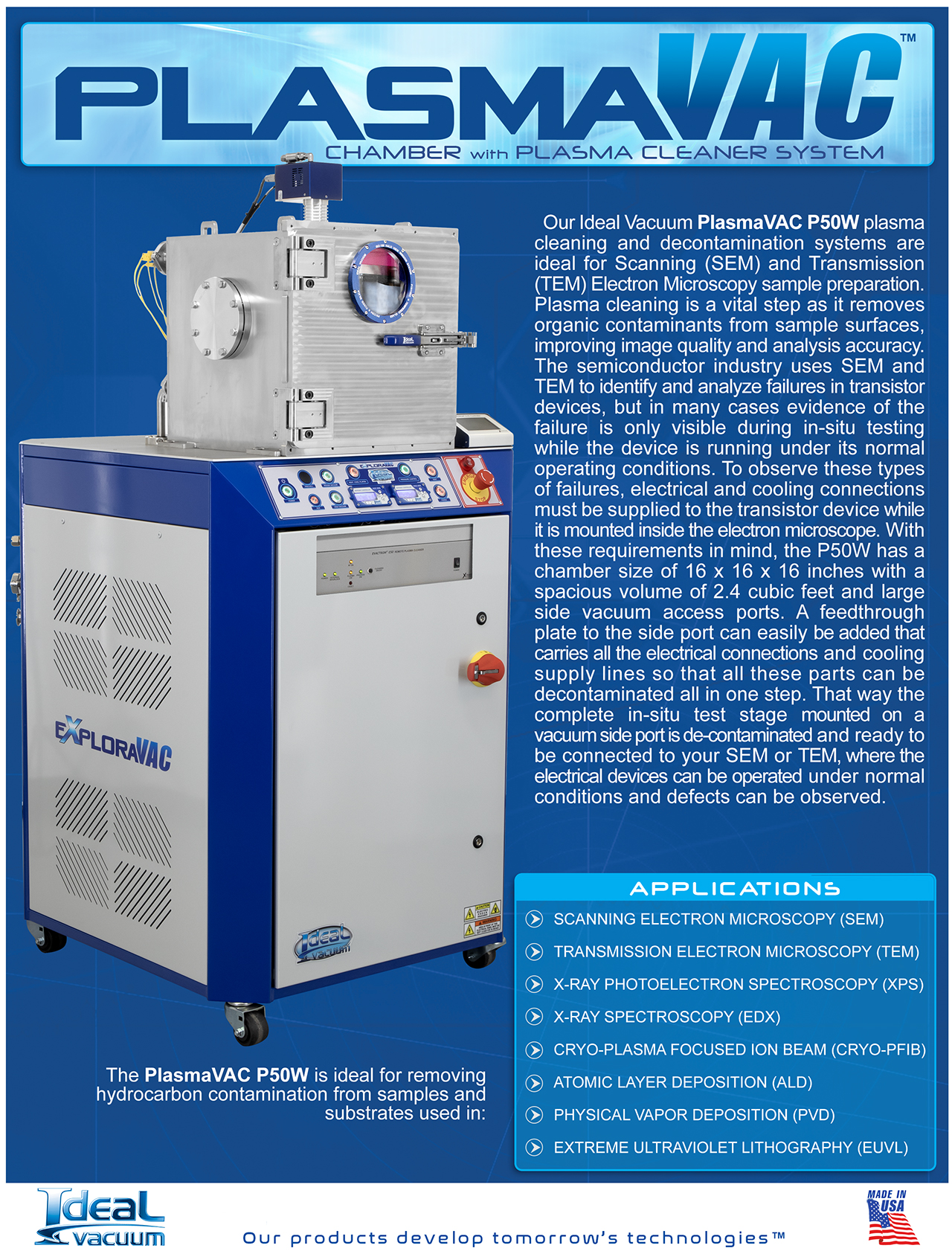
Ideal Vacuum PlasmaVAC P50W Plasma Cleaning & Decontamination System, with Remote Plasma Source
Commonly Used for SEM, TEM, ALD, & PVD Sample and Substrate Preparation.
Our Ideal Vacuum
PlasmaVAC P50W plasma cleaning and decontamination systems are ideal for Scanning (SEM) and Transmission (TEM) Electron Microscopy sample preparation. Plasma cleaning is a vital step as it removes organic contaminants from sample surfaces, improving image quality and analysis accuracy. The semiconductor industry uses SEM and TEM to identify and analyze failures in transistor devices, but in many cases evidence of the failure is only visible during in-situ testing while the device is running under its normal operating conditions. To observe these types of failures, electrical and cooling connections must be supplied to the transistor device while it is mounted inside the electron microscope. With these requirements in mind, the P50W has a chamber size of 16 x 16 x 16 inches with a spacious volume of 2.4 cubic feet and large side vacuum access ports. A feedthrough plate to the side port can easily be added that carries all the electrical connections and cooling supply lines so that all these parts can be decontaminated all in one step. That way the complete in-situ test stage mounted on a vacuum side port is de-contaminated and ready to be connected to your SEM or TEM, where the electrical devices can be operated under normal conditions and defects can be observed.
The
PlasmaVAC P50W is ideal for removing hydrocarbon contamination from samples and substrates used in:
- Scanning Electron Microscopy (SEM)
- Transmission Electron Microscopy (TEM)
- X-ray Photoelectron Spectroscopy (XPS)
- X-ray Spectroscopy (EDX)
- Cryo-Plasma Focused Ion Beam (Cryo-PFIB)
- Atomic Layer Deposition (ALD)
- Physical Vapor Deposition (PVD)
- Extreme Ultraviolet Lithography (EUVL)
The
PlasmaVAC P50W has a remote hollow cathode plasma radical de-contaminator made by XEI Scientific, Inc with model Evactron E50 E-TC. This source offers RF power between 35 to 75 Watts at 13.56 MHz and includes a library of tested recipes and options to change power, cycles, and length of cleaning. The Evactron E50 E-TC has two gas inlet options: a ultrahigh-purity gas inlet filter (3 nm pore size) version to meet the stringent requirements of the semiconductor industry SEMI F38-0699 directive and the precision filter option (0.5 µm pore size) version for general lab conditions. These in-line filters prevent the introduction of particulates from gas feedlines into the plasma stream. Alternate gases which have been tested include O2, CDA, Ar/ H2, Ar/O2, N2/H2, and N2. The use of 100% H2 is not recommended for safety reasons.
PlasmaVAC P50W surface treatment specifications:
- Remote Plasma Source by XEI Scientific
- Model Evactron E50 E-TC
- Power Adjustable Between 35 to 75 Watts
- Max of 50 Watts Continuous Operation
- RF Frequency at 13.56 MHz
- Two Gas Inlet Filter Options: 3 nm & 0.5 µm Pore Sizes
- The 3 nm Pore Sizes Follows Semiconductor Industry SEMI F38-0699 Directive
- Tested With O2, CDA, Ar/ H2, Ar/O2, N2/H2, and N2 Gases.
- Dedicated Evactron User Interface Controller
- Storage Of User Settings
- Recipes, Power, Cycles, and Length of Cleaning
- Front Viewport
- Side Access Vacuum Ports
- Turbo Throttling
- Heated Shelf (60 °C) Mounted Below The Plasma Source
- Heated Shelf Distance Is Adjustable In 1-inch Increments
- 2 Additional Slotted HV Storage Shelves
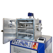
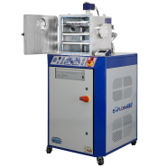
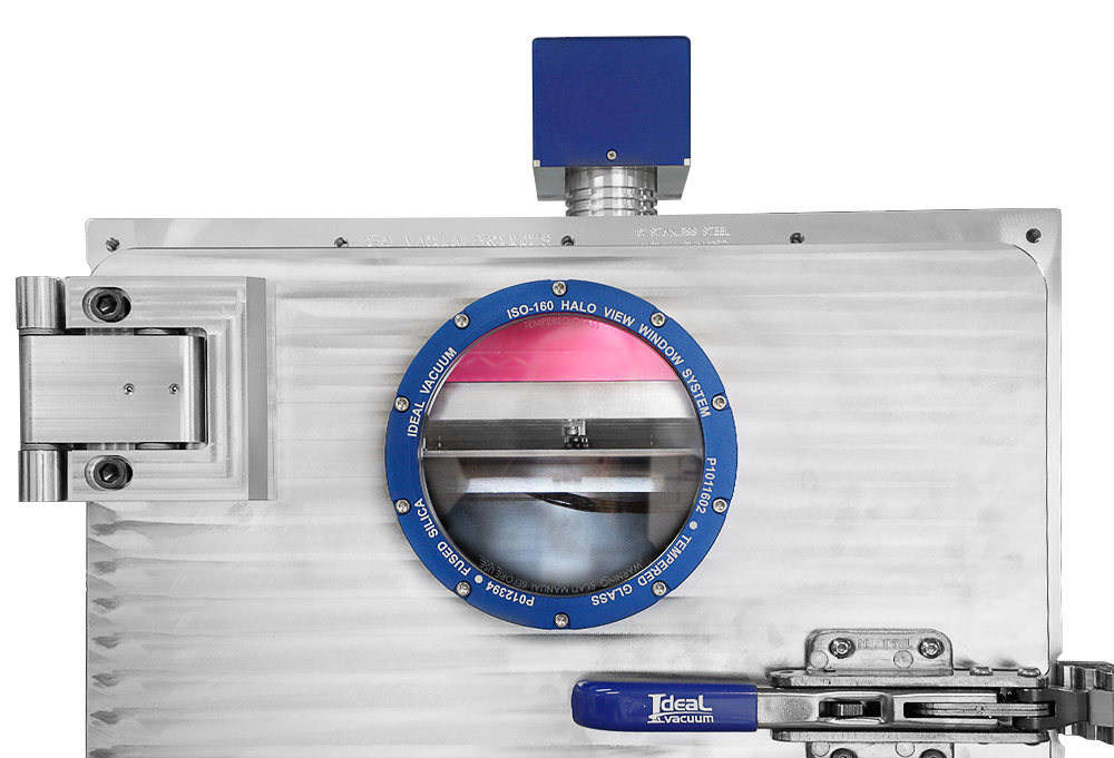
This P50W system includes an Edwards nXR60i dry multistage-roots roughing pump and an undermounted Pfeiffer HiPace 300 turbo pump with TC400 controller. Its features also include atmospheric venting and an integrated Inficon MPG400 combination Pirani & cold cathode inverted magnetron gauge. Chamber vacuum pressure measurements are displayed via a console mounted pressure controller which also allows the user to control the speed of the turbo pump. Included is a heated platen shelf mounted high in the chamber for optimal plasma cleaning of transistor devices or wafers, where temperature is controlled by a separate console mounted controller and is limited to a maximum of 60 °C to prevent burn hazards to the operator. The heated shelf is installed at the optimal distance for cleaning of SEM and TEM samples and is adjustable up or down in 1 inch increments for other applications as needed. Two additional shelves are located below the heated shelf for additional high-vacuum storage space. The Evactron E50 E-TC remote plasma cleaning system is built-into the roof of the chamber and a separate Evactron dedicated interface controller allows the user to easily vary all important cleaning parameters and keep user recipes. The chamber features a hinged stainless-steel door with a viewport and built in polycarbonate filter to protect the user from IR and UV radiation generated by the plasma arc. This PlasmaVAC instrument includes an interlock which does not allow the plasma cleaning system to operate above 1 Torr.
The AutoExplor software option allows a user to control devices from a remote computer while protecting the system. AutoExplor properly sequences pumps and automatically operates the correct valves for a given request. The user can program pressure and temperature setpoints, ramp rates, soak times, and venting. The software provides real-time graphical data streaming so the user can visualize system behavior. AutoExplor maintains an internal preventive maintenance schedule and notifies the user when system service, such as pump maintenance or sensor calibration is due. This helps keep the system at peak operating performance. It also provides fault and error messages along with specific troubleshooting information in the case of a device failure so that the issue can be corrected as soon as possible.
Plasma cleaning is a technique widely used in microscopy, including Scanning Electron Microscopy (SEM) and Transmission Electron Microscopy (TEM), to prepare and decontaminate samples. It effectively removes organic contaminants from sample surfaces, improving image quality and analysis accuracy. Here's how plasma cleaning works for SEM & TEM samples:
1. Principle of Plasma Cleaning
Plasma cleaning uses plasma, a highly ionized gas, to remove contaminants. Plasma is generated by applying a high-frequency electromagnetic field to a low-pressure gas, commonly oxygen, argon, or hydrogen. The process creates ions, electrons, and neutral species that are highly reactive.
2. Removal of Contaminants
In the plasma cleaning process:
- Physical Removal: The energetic ions in the plasma bombard the sample surface, physically sputtering away contaminants.
- Chemical Reactions: Reactive species in plasma can chemically interact with contaminants. For example, oxygen radicals can oxidize organic materials, turning them into volatile compounds that are easily removed.
3. Application in SEM and TEM
For SEM samples:
- Decontamination: Plasma cleaning removes organic residues like fingerprints, oils, and airborne particulates that can obscure details or interfere with electron beams.
- Improved Imaging: By cleaning the surface, plasma treatment reduces charging effects and enhances the resolution and contrast of SEM and TEM images.
- Enhanced Resolution and Contrast: A clean sample surface allows for better interaction between the electrons and the sample, which is critical for achieving high-resolution and high-contrast images in SEM and TEM.
- Preparation for Coating: It's often used prior to applying conductive coatings to non-conductive samples, ensuring the coating adheres well and is uniform.
4. Advantages of Using Plasma Cleaning
- Gentle on Samples: Unlike chemical cleaning methods, plasma cleaning is generally non-destructive to the sample surface.
- Fast and Efficient: The process can take from a few minutes to an hour, depending on the contamination level and the sample size.
- Versatile: Effective on a variety of materials, including metals, ceramics, and biological samples.
Electron microscopes, particularly Scanning Electron Microscopes (SEM) and Transmission Electron Microscopes (TEM), are vital tools in the semiconductor industry for identifying and analyzing failures in transistor devices. The ability of these microscopes to provide high-resolution images at the nanoscale allows for detailed examination of semiconductor materials, structures, and devices. Here’s how electron microscopes are used in this context:
1. High-Resolution Imaging
- SEM: SEMs are used to visualize the surface topography and composition of transistor devices. They can identify surface defects, layer thickness variations, and structural abnormalities that may lead to transistor failure. The backscattered electron (BSE) mode can differentiate between materials based on atomic number contrast, which is useful for inspecting the composition and distribution of materials in the device.
- TEM: TEM provides even higher resolution than SEM and can image at the atomic level. This is crucial for viewing internal structures of the transistors, such as crystal lattice defects, dislocations, and interface anomalies between different materials.
2. Failure Analysis
- Defect Analysis: Electron microscopes can detect and analyze defects that are not visible with less powerful microscopes. These include voids, cracks, and foreign material inclusions within the transistor.
- Material Analysis: Energy-Dispersive X-ray Spectroscopy (EDX) capabilities in electron microscopes can be used to perform elemental analysis and confirm the chemical composition of materials. This helps in understanding issues like contamination or material degradation.
3. Fault Localization
- Circuit Edit and Debugging: Focused Ion Beam (FIB) systems, often combined with SEM, are used for circuit edit and failure analysis. They can mill away materials at specific locations to expose the internal sections of a transistor or to repair and modify circuits at the nanometer scale.
- Physical Sectioning: For internal defects or failures, FIB can be used to cut cross-sections of the devices. These cross-sections can then be imaged under SEM or TEM to analyze the layer structures and interface quality.
4. Electrical Characterization
- Voltage Contrast in SEM: This technique is used to identify electrical activity in semiconductor devices. It can show which parts of the transistor are electrically active and which are not, indicating potential areas of failure.
5. Dynamic Testing
- In Situ Testing: Some electron microscopes are equipped to perform in situ electrical testing where the device can be observed under operating conditions. This can be instrumental in identifying dynamic failure mechanisms such as electromigration or thermal degradation.
